By now, I have more experience with designing boards using EAGLE PCB. So I will do my best to explain here the steps you need to take.
Download libraries
The fab library here has all the components. Download the file, and place in you EAGLE libraries folder. After that, open the library manager, and under "avilable" you should see the file, select it and click "use"
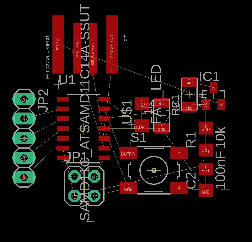
Draw the schematic.
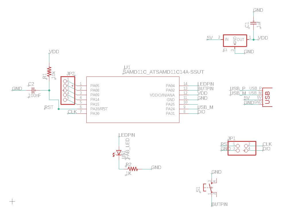
In my case, I started with the SAMD11C chip, you go to add part and look for it in the appropiate library.
The schematic view deals with the part creation, labeling of conections, and the circuit characterization, e.g. the values for resistors, etc. I included the fab library file to the EAGLE settings because those parts are the ones we have on site.
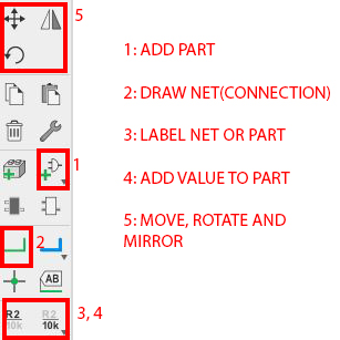
The basic process is to 1) add parts, then 2) connect them, 3) label them 4 add values to resistors, capacitors etc, and you move things around to keep them tidy. Labels help a lot because identical labels are connected automatically. for example a net with GND label will automatically connect to all other labeled GND.
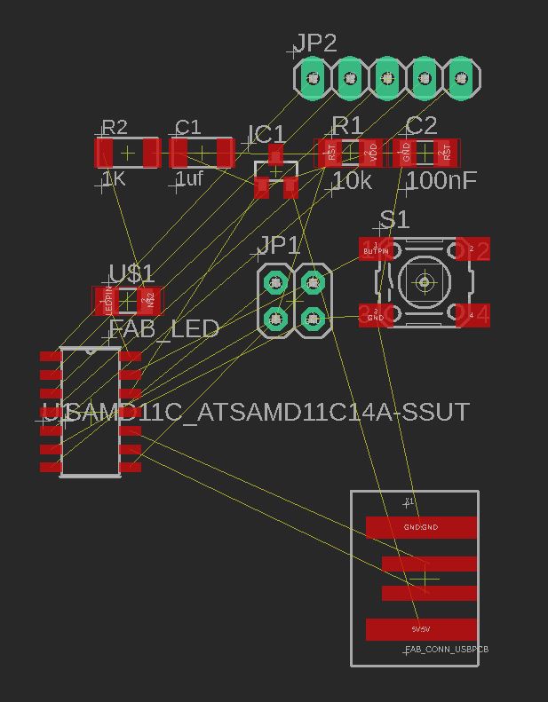
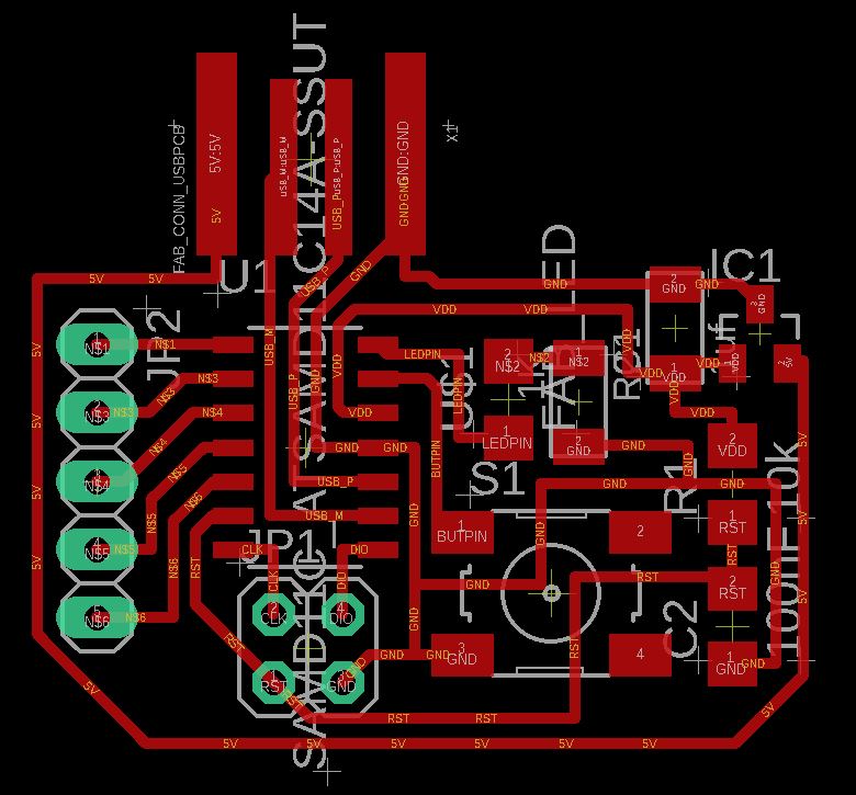
After doing the schematic, you have to make the board design. The connected parts in the schematic will be linked in the board design view. At first, it will be a mess, your job is to place the parts and physically connect the traces. Each part will have its footprint.
What I did was just start copying parts and connections from the programmer, just copying the interface for flashing it, and then adding the LED and button on the available pins. I also added a connector for al the rest of the pins. The LED will go on pin PA04 and the button will go on pin PA02. The button does not need a pull up resistor because the SAMD already has them built-in. Press the board view icon to see the board. It'll be a mess:
You will move and rotate things so that hey're correctly placed. You will move them around quite a bit, and then route the unconnected parts using the "Route Airwire" command.
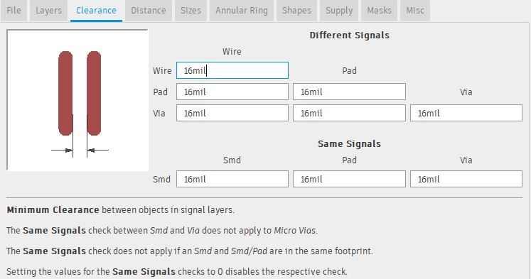
To route you have to configure your design rules. Most important are the separations. Go to Edit>>Design Rules... I set them to 16mil:
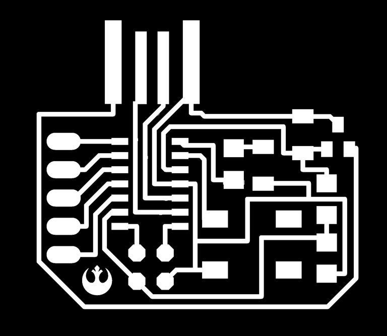
After that just go to file>>>export>>>image and select 1500 dpi. Then select png format and whole window. Make sure you select "monochrome" you should get the two images, traces and interior:
Programming
To program the board you first need a programmer that we made befor. That programmer has a target board connection, which we will use ONLY ONCE to upload the Arduino Bootloader.
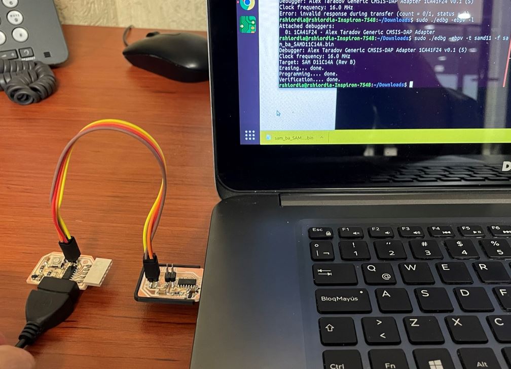
First, connect everything like so:
Then, download the arduino bootloader from Quentin Bolsee .
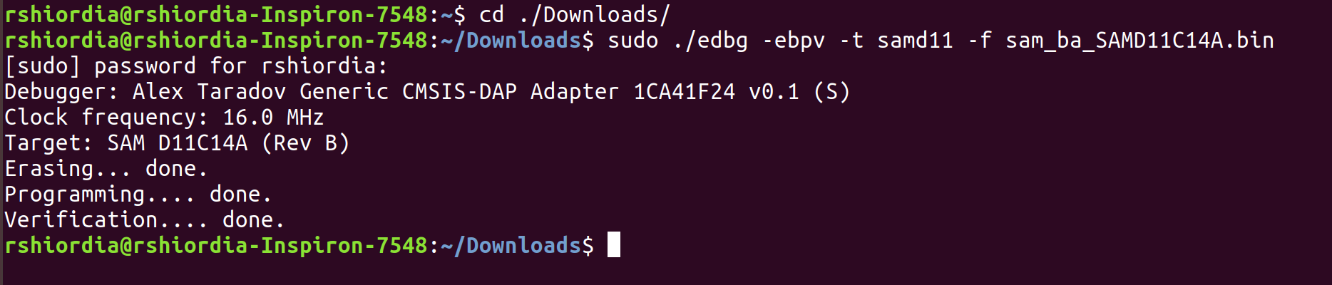
Put the file in the same folder as EDBG and run:
edbg -ebpv -t samd11 -f sam_ba_SAMD11C14A.bin
Once that is done, you will be able to program your board directly from Arduino. Here are the steps:
first, go to file>>> preferences and add the URL for the arduino core that will allow us to select this chip and program it from the Arduino IDE. The URL is this one:
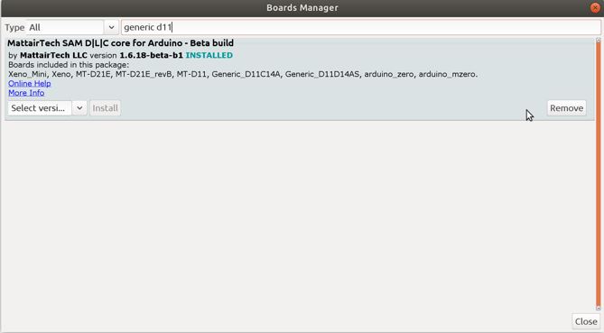
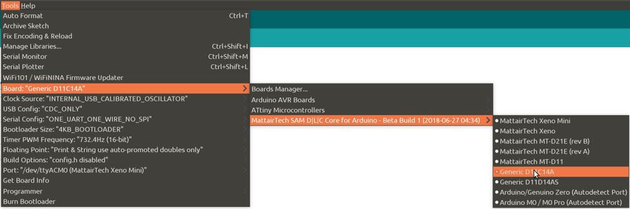
Then, you should add the SAM D|L|C core for Arduino using tools>>board>>>>>boards manager... type generic d11 on the search bar and it should appear. It won't appear unless you add the URL from last step.
Then and only then will you be able to select the board from the tools menu:
Finally... you can now upload code to the board using normal arduino In my case, the first code I uploaded was this:
I used Eagle PCB to design my board. It was a hard process. From the design rules of week 3, the first thing I did was extrapolate the settings for using EAGLE PCB. The first thing is that 1/64" is equal to 16 mil . Thoose were the settings used for the traces.
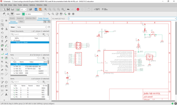
First step was to get the schematic drawn. I started from the schematic on the tutorials page, and added the button, LED, and resistors of the AtTiny 44 board.
This is the schematic.
The schematic view deals with the part creation, labeling of conections, and the circuit characterization, e.g. the values for resistors, etc. I included the fab library file to the EAGLE settings because those parts are the ones we have on site.
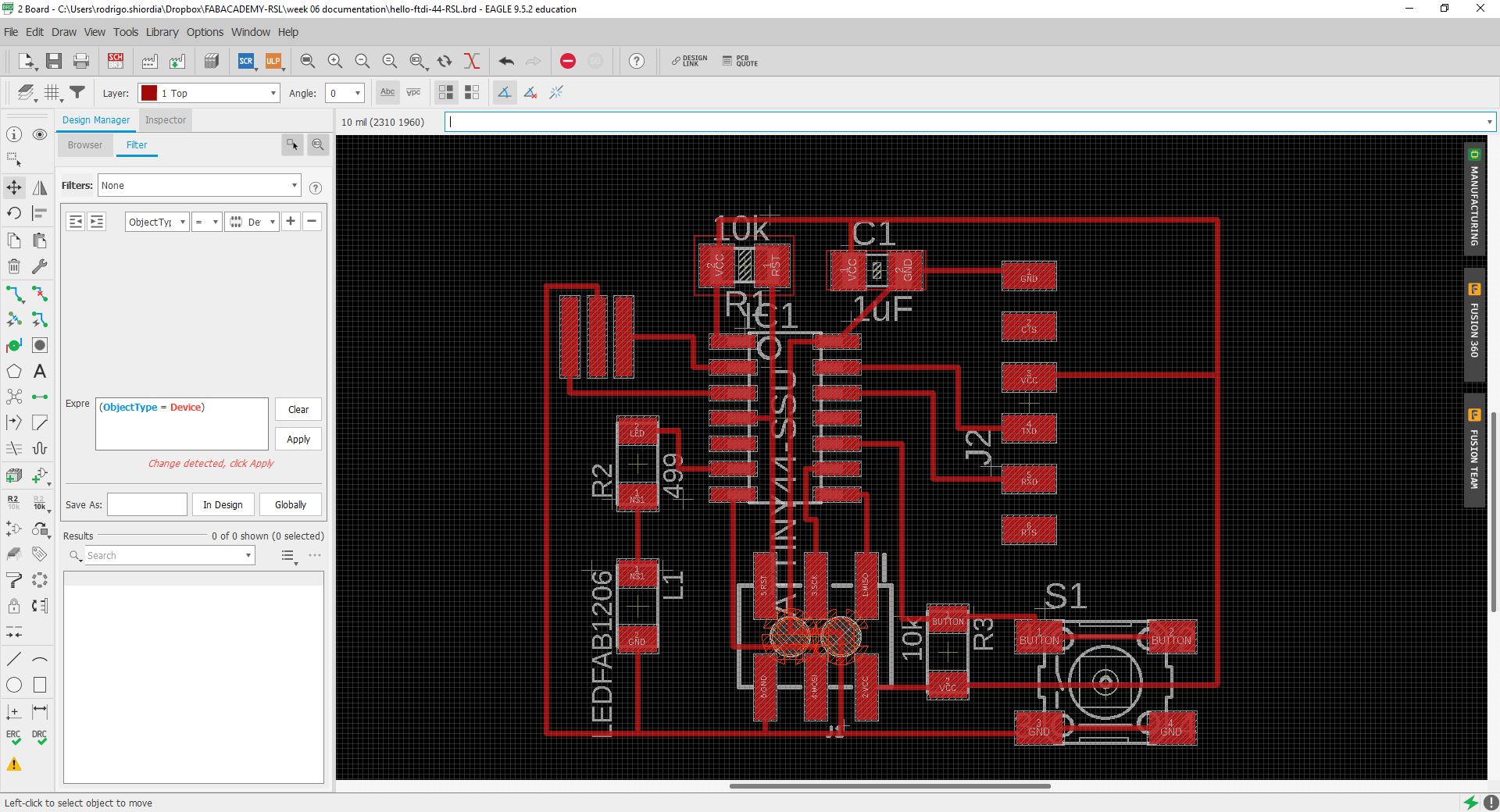
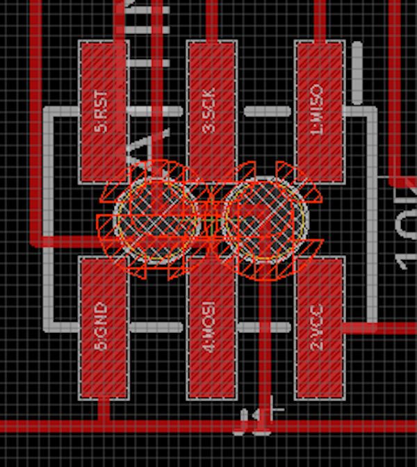
The board was design by copying the design of the Hello Board, and adding a button, two resistors, and the LED. The first thing I did was to put the AtTiny board. Once that was there I added the ISP connection. My main challenge was to avoid collisions and crossings of traces. What EAGLE does is to include "airwires," which you turn to traces that will be milled afterwards. As I said I used 16mil and also I configured the grid to be 5mil so that every time two traces are too close I can check that they have at least 3 squares between them, so that the 1/64" mill can go between them with ease.
One thing I did was to avoid overcrowding of traces. The grid tool described above helped a lot with this. Some re-routing and 45 degree junctions were enough to clear up crowded areas as seen above.
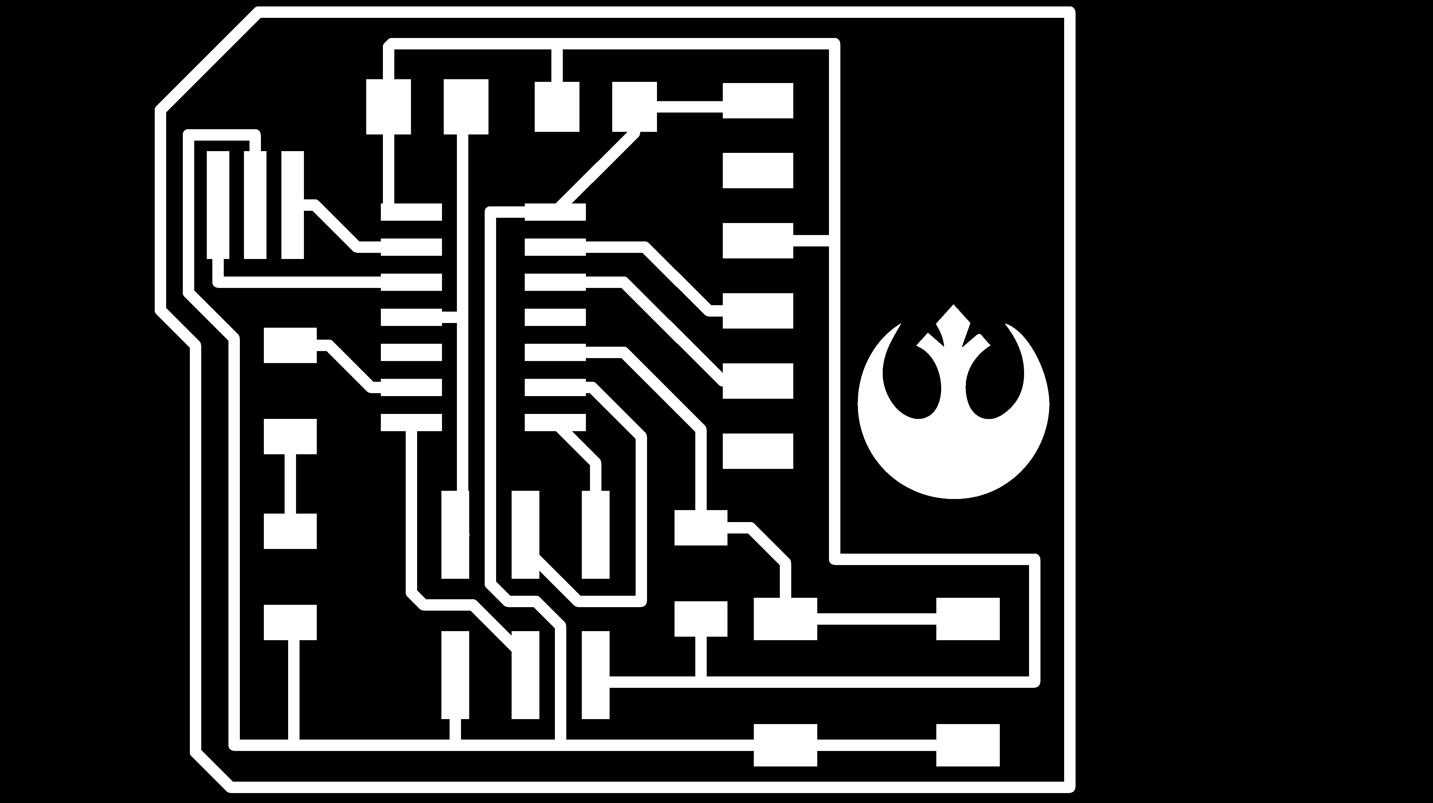
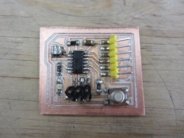
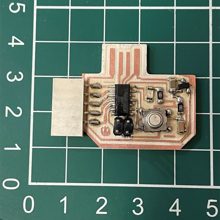
This is the final board. I added the icon so that you know that the force is strong with this one.
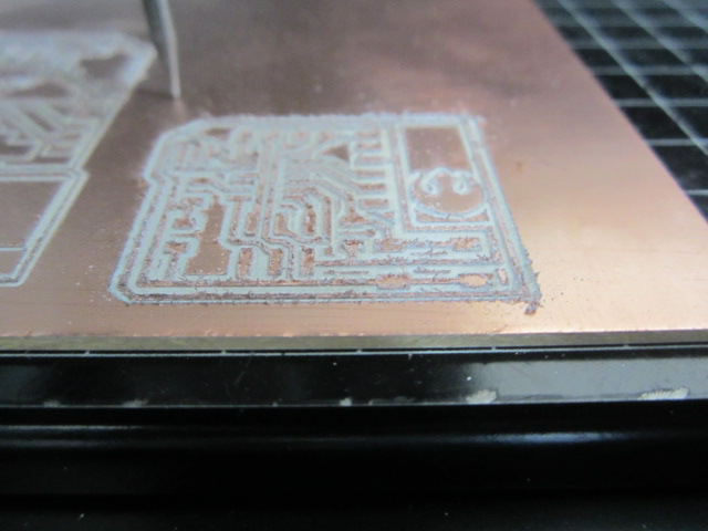
The board milling went smoothly, however I made two boards in case soldering went awry. This proved good foresight on my part.
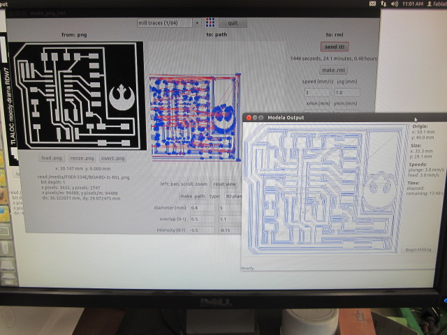
This is the milling of the board in action. We are using an older version of mods, but it works very well.
back to top
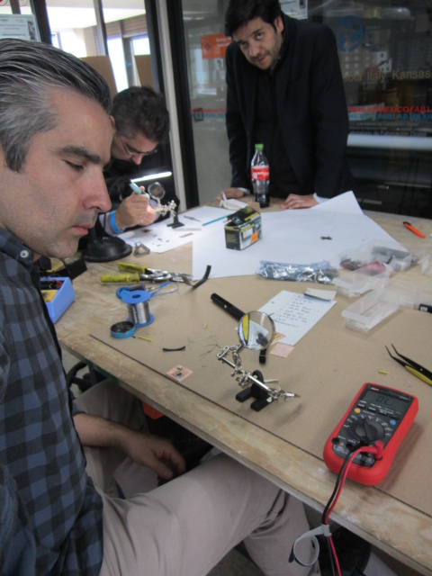
Soldering the components
Soldering setup
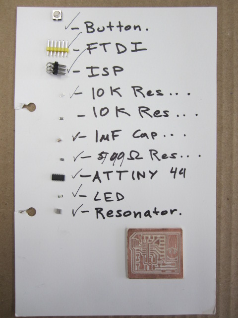
It's important to have good organization when you are soldering, you minimize risk of getting burned withthe iron, and you work better overall. First set up your components on a list:
button check which terminals are the switch
10k resistors no polarity, they have written how many ohms they are. Use multimeter to test resistance if necessary.
LED The LED has polarity so check the side with a green line that's the cathode, it always goes to GND.
AtTiny44 It'll have a small dot on the upper left corner, thiswill orient you to the correct orientation of the IC on the board.
Resonator No polarity, pretty small so be careful when you solder the three connections.
1uF Capacitor No polarity
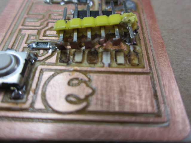
Soldering mistake!
I made a big mistake. While soldering I left the iron for too long on the copper, and apparently the copper dislodged from the board. This was a problem, and the whole FTDi jumper came off.
As you can see, the copper came off, rendering the whole board useless.
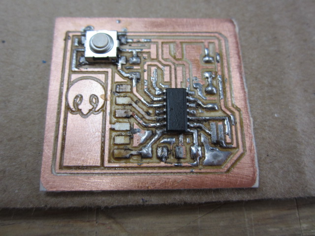
Board 2nd try
This is the final board. I tried not to make the same mistake, and I used the pump and iron to salvage as many parts from the first try. Dislodging the AtTiny from the first board proved difficult. I decided to just use a new one. All the other parts were desoldered from the first try and assembled to this new board.
Connecting and uploading code
This board was tested using a multimeter and all continuity worked. I made many different tests to program it. All the programming and uploading code is documented here
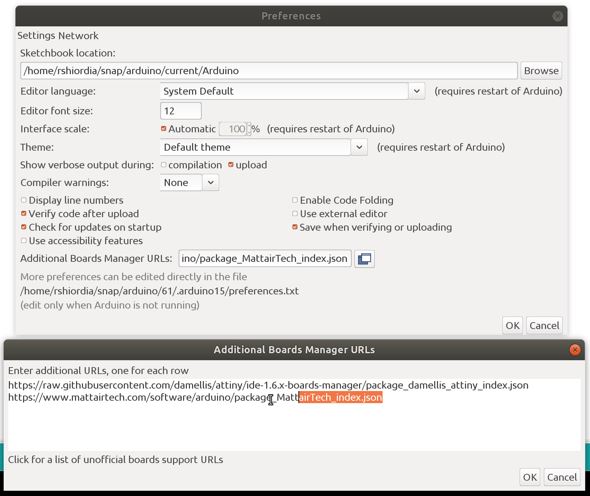 Then, you should add the SAM D|L|C core for Arduino using